How Stealth Technology Actually Works
Most people think stealth means invisible. Like the plane disappears. Like radar just... doesn't see it.
That's not what happens. Stealth is not invisibility. It's a careful, deliberate reduction in how loudly something announces itself to the electromagnetic spectrum. The F-22 isn't invisible to radar. It just looks like a bird. A small one. At the wrong time of day.
Understanding how that works requires going back to what radar actually is, how surfaces scatter electromagnetic waves, and why the shape of a jet (down to the angle of a panel seam) is a national security decision.
What Radar Is Actually Doing
Radar works on a simple principle: send out a pulse of electromagnetic energy, wait for it to bounce back, measure how long it took and how strong the return signal is. From that you get distance, direction, and with enough pulses, velocity.
The key word is bounce. Radar depends on the target reflecting energy back toward the receiver. The more energy that comes back, the easier the target is to detect, track, and lock onto.
The measure of how much energy an object reflects back is called Radar Cross Section, or RCS. It's measured in square meters, but it's not the physical size of the object. It's the effective size of a perfectly reflective sphere that would return the same amount of energy. A large flat metal plate facing directly toward a radar might have an RCS of hundreds of square meters. A metal sphere the size of a marble has an RCS roughly equal to its actual cross-sectional area. A modern stealth aircraft aims for an RCS somewhere around 0.001 m², about the size of a marble, regardless of the fact that it's a 20-meter-long aircraft carrying 18,000 kilograms of fuel and weapons.
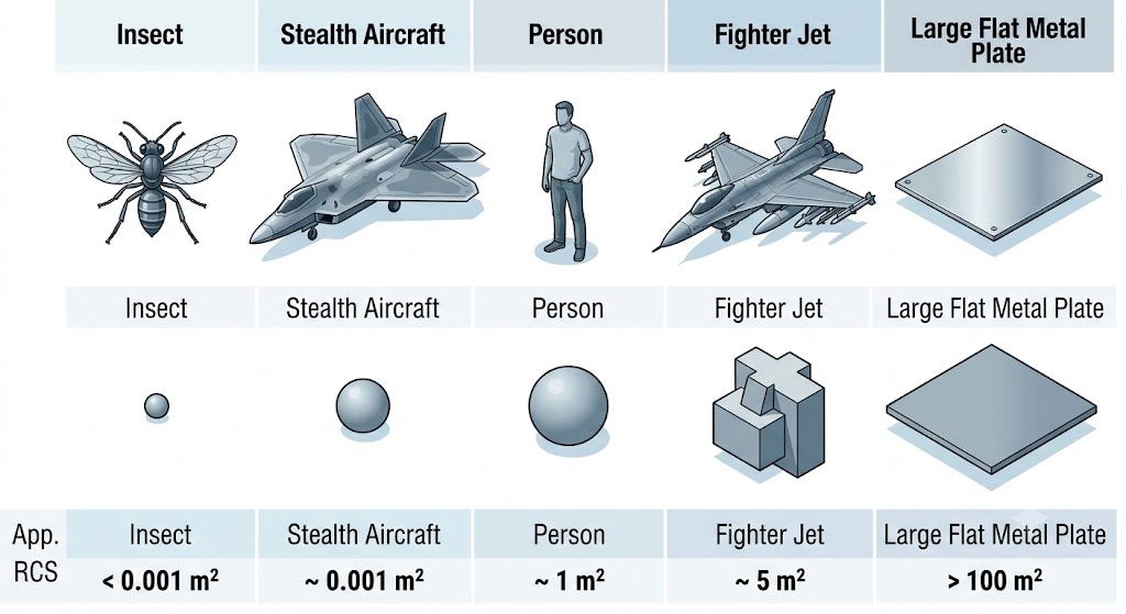
RCS isn't a fixed number. It changes with frequency, with the angle of the incoming wave, with the polarization of the radar signal. A plane that's nearly invisible to an S-band radar might light up on a VHF system. Stealth is always defined relative to a specific threat environment, never in absolute terms.
Two Ways to Reduce RCS
There are fundamentally two approaches to making something harder for radar to detect. You can change its shape so that reflected energy goes somewhere other than back to the radar. Or you can coat it with a material that absorbs the incoming energy before it can bounce back. In practice, every real stealth platform uses both.
Shaping: Directing the Reflection Away
When an electromagnetic wave hits a surface, it reflects. The angle of reflection equals the angle of incidence, the same rule as light on a mirror. Stealth shaping exploits this: if you orient all your surfaces so that the specular reflection goes off at an angle that doesn't point back toward the radar, the return signal is dramatically reduced.
This is why the F-117 Nighthawk looked the way it did: a collection of flat, angular facets arranged so that incoming radar energy got scattered off in specific directions rather than reflected back to the source. It looked like something assembled from broken glass. That wasn't aesthetic. Every angle was a calculated decision about where the reflected energy would go.
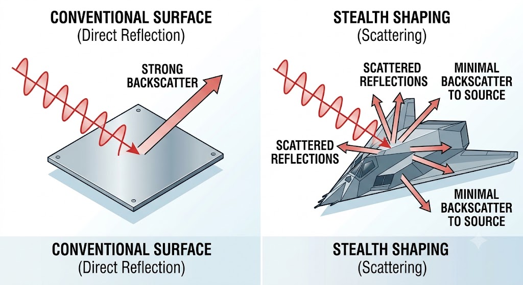
The B-2 Spirit took a different approach. Instead of flat facets, it uses smooth, continuously curved surfaces (flying wings with blended edges) that spread the reflected energy over a very wide angular range rather than scattering it into discrete lobes. Curved surfaces don't eliminate reflection, but they dilute it. Neither approach is "better." They represent different engineering tradeoffs between manufacturing complexity, aerodynamic performance, and the specific radar frequencies you're trying to defeat.
There are limits to what shaping can do. Edges, inlets, gaps between panels, weapons bay doors: all of these create radar returns that shaping alone can't eliminate. A perfectly shaped aircraft with metal skin still reflects. That's where materials come in.
Absorption: Killing the Signal Before It Returns
The other approach is to build surfaces that absorb incoming electromagnetic energy rather than reflecting it. These are broadly called Radar Absorbing Materials, or RAM. The idea is conceptually simple: when the wave hits, convert its energy into heat instead of letting it bounce back.
Early RAM was exactly what it sounds like: rubber or foam material loaded with carbon black or iron particles, applied to surfaces as a coating. It works on the same principle as a black surface absorbing visible light rather than reflecting it. The lossy particles in the material interact with the oscillating electric and magnetic fields of the incoming wave and dissipate the energy as thermal losses.
The problem with early RAM was thickness. To get meaningful absorption, you needed meaningful material thickness, sometimes several centimeters. At microwave frequencies, the wavelengths involved are in the centimeter-to-meter range, and effective absorption requires the material to be on the order of a quarter-wavelength thick. At 10 GHz, a quarter wavelength is about 7.5 mm. That's manageable. At 1 GHz, a quarter wavelength is 75 mm. If you're trying to hide from lower-frequency radar, your absorber starts to weigh more than your aircraft.
This is the central engineering problem of radar absorption: you want the absorber to be thin, lightweight, and broadband, properties that are inherently in tension with each other.
Why Simple Absorption Isn't Enough
To understand why thickness matters, you need to understand how a ground-backed absorber works, because almost all practical radar absorbers use this configuration.
Imagine a thin layer of absorbing material placed over a conducting ground plane (the metal skin of an aircraft). An incoming electromagnetic wave hits the absorber, partially enters it, bounces off the ground plane at the back, travels back through the absorber, and partially exits. The wave that exits is the reflected signal, what the radar sees.
If you engineer the absorber correctly, the wave that bounces off the front surface of the absorber and the wave that went in, bounced off the back, and came back out are out of phase with each other. They interfere destructively. The reflected signals cancel. This is essentially the electromagnetic equivalent of noise-canceling headphones.
For this cancellation to work at a specific frequency, the round-trip path through the absorber needs to be exactly half a wavelength, so the returning wave is exactly 180 degrees out of phase with the surface reflection. This sets a fundamental relationship between the absorber's thickness and the frequency it's effective at. Thinner absorber means higher frequency. Getting broadband absorption means either stacking multiple layers (each tuned to a different frequency) or finding a material that has loss spread across a wide frequency range.
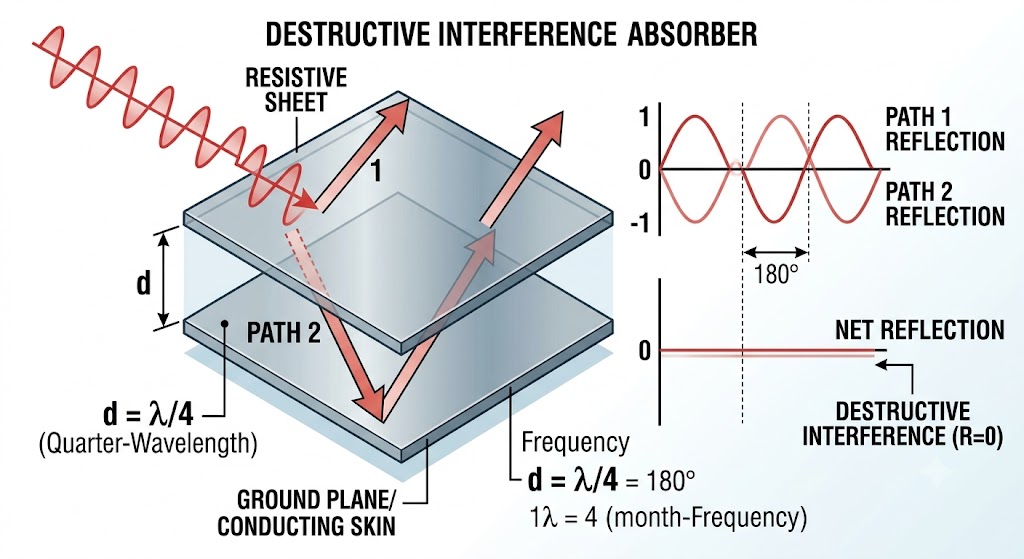
This is the physical reason why early RAM was heavy and thick. Physics imposes it.
Enter Metamaterials and Frequency-Selective Surfaces
The shift that changed this field was moving from bulk absorbing materials to structured surfaces: materials where the electromagnetic behavior comes not from the material chemistry but from the geometry of tiny repeating patterns engineered at sub-wavelength scales. These are broadly called metamaterials or, when designed as planar sheets, frequency-selective surfaces (FSS).
The idea was first proposed cleanly in 1944 by Winfried Dallenbach: a single thin resistive sheet placed a quarter-wavelength in front of a ground plane can achieve near-perfect absorption at the design frequency if the sheet's surface resistance is matched to the impedance of free space (377 ohms). This is the Salisbury screen. It's elegant, it works, and it has one problem: it only absorbs effectively at one frequency (and its harmonics), and the quarter-wavelength spacing still dictates the thickness.
FSS absorbers solve the bandwidth problem by replacing the simple resistive sheet with a patterned surface. Instead of a uniform resistive layer, you have a periodic array of carefully shaped conducting or resistive elements (patches, rings, crosses, Jerusalem crosses, whatever geometry the designer chooses). Each element behaves as a tiny resonator. By designing elements with slightly different resonant frequencies, or by coupling multiple resonances together, you can spread the absorption over a much wider band.
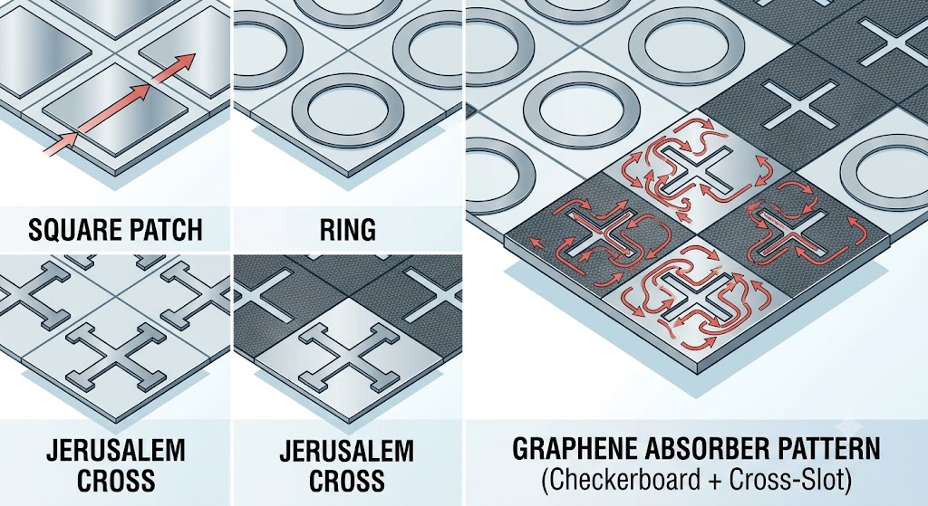
Crucially, the resonant frequency of the FSS element depends on its geometry, not just the material it's made of. This gives designers a new degree of freedom: you can tune the absorption frequency by adjusting the shape, size, and spacing of the elements rather than by changing material thickness. This makes it possible, in principle, to get broadband absorption in a layer that's much thinner than a naive material approach would require.
Impedance Matching: The Real Engineering Problem
All of this comes down to one underlying concept: impedance matching.
Electromagnetic waves travel through free space with a characteristic impedance of about 377 ohms. When a wave hits a surface, how much gets reflected versus absorbed depends on how well the surface's impedance matches free space. Perfect impedance match means no reflection: all the energy enters the material. Perfect mismatch (like hitting a perfect conductor) means total reflection: all the energy bounces back.
For a ground-backed absorber, the normalized impedance you want to present to free space is exactly 1 + j0, with the real part equal to one (matching free space) and the imaginary part equal to zero (no reactive component). If you can engineer a surface with that impedance at the frequencies you care about, reflection drops to zero. Your target goes quiet.
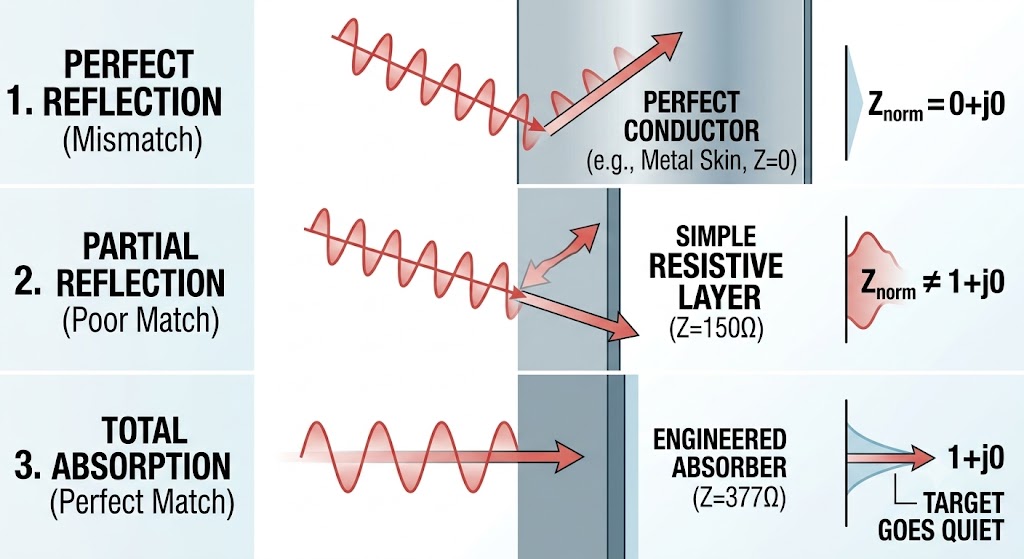
The normalized input impedance of an absorber can be retrieved from its reflection coefficient S11:
Z_norm = (1 + S11) / (1 - S11)
When |S11| approaches 0 (perfect absorption), Z_norm approaches 1 + j0. When you plot the real and imaginary parts of Z_norm against frequency and watch them converge to 1 and 0 respectively, you know your structure is working. This is the standard diagnostic for any absorber design: not just "does the absorption curve look good" but "does the impedance response tell the right physical story."
The Modern Toolkit: Graphene and ITO
Recent FSS absorber research has moved toward resistive materials that can be deposited as ultra-thin sheets, most importantly graphene and ITO (indium tin oxide).
Graphene at microwave frequencies behaves as a zero-thickness resistive sheet with a tunable surface resistance. Its surface conductivity in the microwave regime is dominated by intraband transitions, meaning you can model it simply as a sheet resistance, typically in the range of tens to hundreds of ohms per square depending on the number of layers and doping. This is exactly the kind of controlled ohmic loss you want for an absorber top layer: you're introducing loss to dissipate incoming energy, but doing it in a geometry-defined way through the FSS pattern.
ITO (indium tin oxide) is a transparent conducting oxide. It has much lower sheet resistance than graphene, typically single-digit ohms per square, making it a good choice for the ground plane backing. It suppresses transmission through the structure (acting like the conducting backplane) while being optically transparent, which has applications in surfaces where visual transparency matters alongside radar absorption.
A graphene/quartz/ITO stack (patterned graphene on top, fused quartz substrate in the middle, continuous ITO sheet at the back) is a structurally simple three-layer configuration that can achieve the full requirements for a practical FSS absorber. The graphene layer provides controlled ohmic loss and geometric resonance, the quartz substrate provides the spacing and dielectric environment, and the ITO backing suppresses transmission and enables the destructive interference condition.
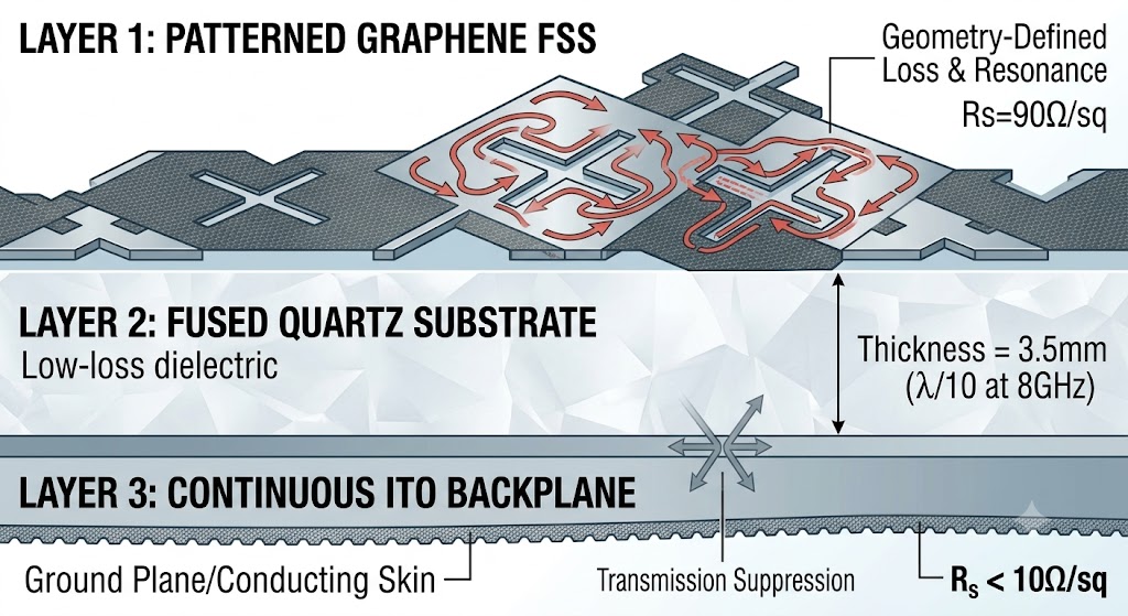
The design parameters that matter most in such a structure:
Graphene sheet resistance controls how much loss is introduced at resonance. Too low and the structure reflects; too high and it doesn't absorb enough. There's an optimal range, typically around 90 ohms/sq for X-band absorbers, where the tradeoff is balanced. Get it wrong by 30 ohms/sq in either direction and the absorption curve degrades noticeably, especially at the band edges.
ITO sheet resistance controls transmission suppression. Below about 10 ohms/sq, the curves are nearly coincident: the ITO acts as a good approximation of a perfect conductor for practical purposes. This gives fabricators some tolerance. The graphene resistance needs tight control, but the ITO can vary within a range without significantly affecting performance.
Unit cell geometry (the size, shape, and pattern of the graphene FSS elements) controls where resonance occurs and how broad the absorption band is. Cross-shaped slots cut into the graphene patches increase the effective electrical length of the current path, generating multiple closely-spaced resonant modes that merge into a single broadband absorption peak. This is the standard technique for bandwidth enhancement in FSS absorbers.
Substrate thickness sets the electrical path length and constrains the minimum absorber thickness. For X-band (8 to 12 GHz), achieving broadband absorption in a substrate around 3 to 4 mm thick corresponds to roughly one-tenth of a wavelength at the lower band edge, significantly thinner than the quarter-wavelength Salisbury screen baseline.
How You Actually Evaluate One
Simulating an absorber in CST Microwave Studio (the standard tool for this kind of work) uses periodic boundary conditions to model an infinite array of unit cells from a single element. Floquet ports excite the structure with plane waves at specified incidence angles and polarizations. The output is S-parameters: S11 (reflection) and S21 (transmission). From these you compute absorption:
A(f) = 1 - |S11|² - |S21|²
For a ground-backed structure, S21 is approximately 0 across the band (the ITO prevents transmission), so absorption simplifies to:
A(f) ≈ 1 - |S11|²
Beyond the absorption curve, you look at several things.
Angular stability: does the absorber work when the incoming wave hits at 15, 30, or 45 degrees? Real targets don't always face the radar head-on. Most FSS absorbers maintain performance up to about 45 degrees of oblique incidence. Beyond that, changes in effective impedance and propagation path through the dielectric start degrading the response. At 60 degrees, you typically see pronounced reduction near the band edges, especially for TE polarization.
Polarization insensitivity: does it work equally for TE and TM polarized waves? This depends on the symmetry of the unit cell. A diagonally symmetric checkerboard pattern is polarization-insensitive at normal incidence because the geometry presents the same effective response to both polarizations.
Surface current and power loss distribution: where is the energy actually going? Surface current plots at resonant frequencies show you whether the intended current paths are being excited. Power loss density maps confirm that energy is being dissipated in the resistive layer and substrate rather than radiating or transmitting. These diagnostics tell you whether the absorption mechanism is what you think it is, not just that the numbers look right but that the physics is right.
Finite-panel RCS: for stealth applications specifically, the absorber's performance on a real finite-size panel matters. A unit-cell simulation assumes an infinite periodic array. A real aircraft panel has edges, corners, and a finite extent. Simulating a 10x10 panel array and examining the 3D RCS pattern at different frequencies tells you about the qualitative scattering behavior, whether the panel redistributes reflected energy spatially rather than concentrating it back toward the radar.
The Gap Between Simulation and Reality
Everything described above is simulation. The field has become very good at simulating absorbers. Getting them to behave the same way in fabrication is a different problem.
Sheet resistance of graphene varies depending on growth method, number of layers, substrate interactions, and even humidity. The nominal 90 ohms/sq value used in design might drift plus or minus 20 ohms/sq in a real deposited film. Substrate thickness tolerances, alignment between layers in a multi-layer stack, pattern dimensional accuracy in photolithography or inkjet printing: all of these shift the impedance-matching condition and can move the absorption band or reduce the peak absorption.
This is why sensitivity analysis matters. Before fabricating anything, you sweep the design parameters around their nominal values and observe how much the absorption response degrades. A well-designed absorber is tolerant to small manufacturing variations. Its performance doesn't fall off a cliff if the graphene sheet resistance is 85 instead of 90 ohms/sq. A poorly designed absorber might drop below the 90% absorption threshold if the substrate comes out 0.1 mm thinner than specified.
The current state of the art in graphene-based FSS absorbers is achieving continuous absorption above 90% across the full X-band (8 to 12 GHz) in a structure under 4 mm thick, approximately one-tenth of a wavelength at 8 GHz, with stable performance up to 45 degrees of incidence and polarization insensitivity at normal incidence. That's in simulation. The experimental side (free-space characterization with horn antennas and a vector network analyzer) remains an active area of ongoing validation work.
Where This Led Me
I didn't come to any of this through aerospace engineering or a radar systems course. I came through a summer research project on wristband sensors and antenna optimization, which somehow cascaded into a second project on metamaterial absorbers.
The graphene FSS absorber I worked on (a checkerboard graphene/quartz/ITO structure with cross-shaped slot loading, simulated in CST for X-band stealth applications) came directly from the antenna physics intuition I'd built on the RFID side of the wristband project. The tools were the same: CST, S-parameter analysis, impedance extraction. The vocabulary was the same: surface resistance, substrate dielectric constant, resonant modes. The questions were just pointed in a different direction. Instead of "how do we radiate efficiently," the question became "how do we absorb efficiently."
They're the same problem, solved in opposite directions.
That inversion, from trying to get energy out to trying to trap energy in, is something I think about a lot. The physics doesn't care about your application. Maxwell's equations don't know if they're describing a life-saving wristband sensor or a surface designed to make a jet invisible to radar. The engineer decides what to do with the tools. The tools are the same.
Stealth isn't magic. It's impedance matching. It's structured loss. It's the careful, deliberate engineering of how electromagnetic energy interacts with a surface, frequency by frequency, angle by angle, polarization by polarization. It is unglamorous in its details and remarkable in its outcomes.
And now, whenever I see an angular aircraft silhouette on the news, I think about S11 curves and sheet resistance tolerances instead of whatever the reporter is saying.
That's probably a sign the summer worked.